|
LTCC LAB |
||||||||||||||||||||||||||||||||||||||||||||||||||
| Home |
LTCC- Low Temperature Co-fired Ceramic process and parameters (typical) LTCC fired Dielectric Constant @ 3GHz 7.8 Loss Tangent @ 3 GHz 0.006 DF (Dissipation Factor) @ 10 MHz 0.15% I R (Insulation Resistance) @ 100 V DC > 1012 Meg ohms Ceramic Breakdown Voltage V/25µm > 1000V LTCC Shrinkage X, Y 12.2%, Z 15% LTCC Thermal Conductivity W/mk 3.3 Thermal expansion of LTCC (25°C-300°C) 5.8ppm/°C Young's modulus GPa 120 Flexural Strength MPa 320 LTCC Density g/cm3 3.1 Surface Roughness µm 3.3 Typical LTCC Via Diameter is 4 to10mils, Via cap 9 mils (Minimum). Conductors Print, Line Width 6 mils, Line space 6 mils (Minimum). Cofired Inner Layer Conductor 100% Silver (Ag). Cofired Top Layer Conductor Pd/Ag, Solderable termination, or Gold. LTCC Green and fired tape thickness.
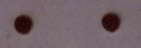
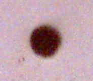
Typical Design Rules for LTCC. (LTCC LAB can change the Design rules to meet customer specifications) 4 mils Vias
|
|||||||||||||||||||||||||||||||||||||||||||||||||